Advanced 3D microfabrication with cutting-edge laser technology.
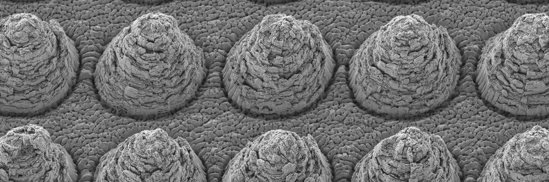
In our research and development projects, we focus on:
Subtractive 3D microfabrication
Development of ultra-short pulse lasers, beam delivery systems, and Industry 4.0 technologies
Additive manufacturing technologies, as well as micro-cutting and micro-joining processes
These areas are among the fastest-growing applications in industrial laser technology and are closely interlinked. The development of new products and manufacturing technologies would not be conceivable without laser microfabrication in future markets such as renewable energy, microelectronics, information technologies, medical technology, and additive manufacturing technologies.
Material processing with ultra-short laser pulses
Ultra-short laser pulses refer to lasers with pulse durations ranging from a few hundred femtoseconds (fs) to picoseconds (ps). Due to their extremely short pulse durations and relatively high pulse energies, these laser pulses reach peak powers in the megawatt range. The average power of currently available industrial lasers reaches a few to several hundred watts due to their high pulse repetition rates. When the laser beam is sufficiently focused on the material surface, the intensity can reach many gigawatts per square centimeter.
Unlike lasers with thermal pulses (ns to ms), material removal does not rely on thermal effects (melting, evaporation) but occurs through a direct transition of the material from solid to gas. This process is explained, among other mechanisms, by multi-photon absorption induced by nonlinear effects caused by the high laser intensity.
The result is minimal thermal load on the material being processed. Melting, thermal stresses, and microstructural changes are largely avoided. Therefore, material removal with ultra-short pulses is often referred to as “cold” material processing.
Combined with the high beam quality achieved by modern lasers, these conditions create an almost ideal tool for microfabrication. Depending on the wavelength, virtually all technical materials can be processed, including metals, crystals, glass, ceramics, as well as organic materials, plastics, and composites.
Process development
We develop and implement industrial 3D microstructuring processes and micro-drilling techniques.
For process investigations, the institute’s laboratory facilities can be utilized. The institute is equipped with a fully equipped materials science laboratory featuring SEM/EDX, microscopy, metallography, surface profile and roughness measurement, as well as various testing machines for both non-destructive and destructive material testing (tensile, compression-tensile testing machines, Charpy impact tests, etc.).
Equipment and Facilities
The laser laboratory is equipped with several picosecond (ps) laser sources from the manufacturers JDSU TIME BANDWIDTH PRODUCTS and TRUMPF:
2 × JDSU TBWP “Duetto”
Power: 5–15 W (wavelengths: 1064 nm, 533 nm, 355 nm)1 × TRUMPF TruMicro 5050
Power: 50 W (wavelength: 1064 nm)
The lasers are integrated into CNC axis systems. Beam delivery is performed via digital scanners, which ensure highly precise, repeatable processing even at high pulse repetition rates of several MHz. The laboratory is also equipped with a high-speed rotary optic, enabling the production of ultra-precise micro-drillings.
Additionally, the laser laboratory has various Q-switched nanosecond (ns) laser systems with different wavelengths, designed either as laboratory setups or fully integrated production systems.
Beyond the laser sources, the lab is equipped with measurement and analysis systems for power and beam characterization.
Contact

Prof. Dr. Ronald Holtz
- Phone
- +41 56 202 83 58 (Direct)
- ronald.holtz@fhnw.ch